Tech:Optical bell: Difference between revisions
PhilmacFLy (talk | contribs) m PhilmacFLy moved page Tech chaos optoring to Tech:Opitcal bell |
Typo fix in explanation. |
||
| (4 intermediate revisions by 2 users not shown) | |||
| Line 1: | Line 1: | ||
At the [[Events:GPN16|GPN16]] the plan was to put field phones in all lecture halls, close to the speaker desks. To be allowed to do so, the requirement was that these phones should not disturb any lectures by loud ringing. So the phones were silenced (TODO: link to description) and equipped with the optical ring indicator described below, before deployment. | At the [[Events:GPN16|GPN16]] the plan was to put field phones in all lecture halls, close to the speaker desks. To be allowed to do so, the requirement was that these phones should not disturb any lectures by loud ringing. So the phones were silenced (TODO: link to description) and equipped with the optical ring indicator described below, before deployment. | ||
[[File:Optoring_schem.png|center|schematic]] | [[File:Optoring_schem.png|center|schematic]] | ||
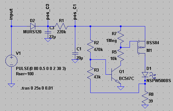
The circuit is shown in the schematic above. The diode D2 rectifies the positive portion of the input ringing voltage and charges up the capacitor C3. Of course the negative portion could have been used equivalently, with the diode in correct polarity connected to the negative side of C3. The maximum peak voltage observed at C3, with heavy cranking at a field phone, was about 150V. As a second stage, the capacitor C1 is now "slowly" charged form C3 trough the resistor R1. Voltage at | The circuit is shown in the schematic above. The diode D2 rectifies the positive portion of the input ringing voltage and charges up the capacitor C3. Of course the negative portion could have been used equivalently, with the diode in correct polarity connected to the negative side of C3. The maximum peak voltage observed at C3, with heavy cranking at a field phone, was about 150V. As a second stage, the capacitor C1 is now "slowly" charged form C3 trough the resistor R1. Voltage at C1 will rise until the base voltage of Q1, generated from C1 voltage through the divider formed by R2 and (R3+R8), is high enough to make Q1 conduct and turn on M1. The moment M1 turns on, there is a significant amount of current that starts flowing through the LED D1 and R8. The now present voltage drop over R8 will additionally feed the base of Q1 and ensures that it stays conducting until the LED current has subsided. C1 will quickly discharge into the LED, making it flash very briefly, for about 2ms, but with high brightness. When C1 voltage has fallen and the LED current has also decreased, Q1 is no longer conducting and M1 also will return to non conducting mode. As long as there is still enough charge in C3, C1 is again charged up via R1 and the next led flash is initiated. The time required for C1 charge up will increase with falling C3 voltage. This results in a continuously slowing down flashing of the LED. | ||
[[File:opotring_sim_full.png|600px|center|simulation]] <br /> | [[File:opotring_sim_full.png|600px|center|simulation]] <br /> | ||
[[File:opotring_sim_blitz.png|600px|center|simulation - single LED flash]] | [[File:opotring_sim_blitz.png|600px|center|simulation - single LED flash]] | ||
| Line 12: | Line 10: | ||
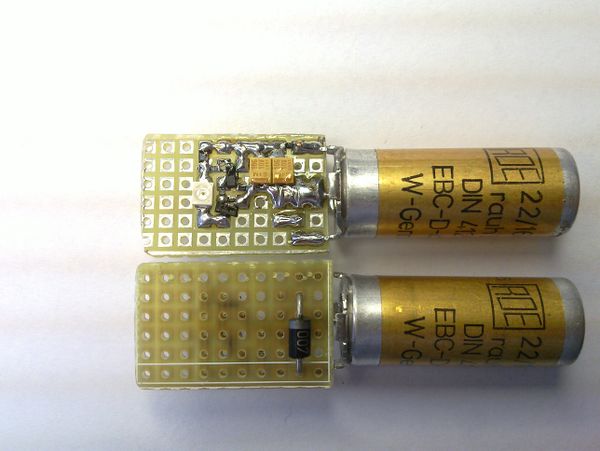
The measurement results of the actual built units match pretty well with the simulation. The voltage across R8 is perfectly suited for monitoring the LED current with an oscilloscope... | The measurement results of the actual built units match pretty well with the simulation. The voltage across R8 is perfectly suited for monitoring the LED current with an oscilloscope... | ||
[[File:hw_optical_bell.jpg|600px|center|Hardware build of the optic bell circuit.]] | |||
Latest revision as of 03:11, 3 April 2018
At the GPN16 the plan was to put field phones in all lecture halls, close to the speaker desks. To be allowed to do so, the requirement was that these phones should not disturb any lectures by loud ringing. So the phones were silenced (TODO: link to description) and equipped with the optical ring indicator described below, before deployment.

The circuit is shown in the schematic above. The diode D2 rectifies the positive portion of the input ringing voltage and charges up the capacitor C3. Of course the negative portion could have been used equivalently, with the diode in correct polarity connected to the negative side of C3. The maximum peak voltage observed at C3, with heavy cranking at a field phone, was about 150V. As a second stage, the capacitor C1 is now "slowly" charged form C3 trough the resistor R1. Voltage at C1 will rise until the base voltage of Q1, generated from C1 voltage through the divider formed by R2 and (R3+R8), is high enough to make Q1 conduct and turn on M1. The moment M1 turns on, there is a significant amount of current that starts flowing through the LED D1 and R8. The now present voltage drop over R8 will additionally feed the base of Q1 and ensures that it stays conducting until the LED current has subsided. C1 will quickly discharge into the LED, making it flash very briefly, for about 2ms, but with high brightness. When C1 voltage has fallen and the LED current has also decreased, Q1 is no longer conducting and M1 also will return to non conducting mode. As long as there is still enough charge in C3, C1 is again charged up via R1 and the next led flash is initiated. The time required for C1 charge up will increase with falling C3 voltage. This results in a continuously slowing down flashing of the LED.


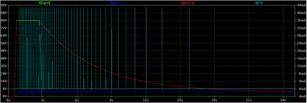
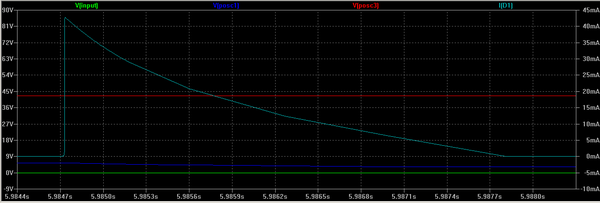
The whole circuit is simulated using LTSpice. The results are shown in the two graphs above. On complete one, where the LED slow down is nicely visible, and a zoom of a single LED flash, where the rapid decrease of LED (D1) current becomes obvious.
The measurement results of the actual built units match pretty well with the simulation. The voltage across R8 is perfectly suited for monitoring the LED current with an oscilloscope...
